

FCBGA Series
分类: FCBGA SeriesFCBGA Technology
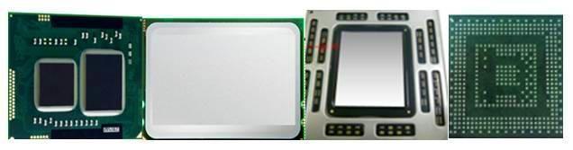
Technology Overview
Flip Chip interconnection, also knownas Controlled Collapse Chip Connection, C4, has been identified as a high performance packaging solution to meet the growing need for products with increased electrical performance, high I/O, and high system reliability as a replacement for conventional wire bond packaging technology. Utilizing whole die area for electrical connection, substrate I/O per unit increases exponentially compared to perimeter wire interconnection technology.
Flip chip interconnect also allows direct connection with on-die power planes which enables increased electrical performance including increased switching speed and more efficient power distribution to the IC performance at lower operating voltages.
Applications
Flip Chippackage technology is considered one of the most established technologyfor high pin count and/or high performance ASICs. Large body FC BGA/PGAs provide package solution for Computing (microprocessors / graphic, server), gaming, high bandwidth networking/Communicationdevices.
Package types
◆ FCBGA Bare die (with or wo stiffener)
◆ FCLGA
◆ FCPGA
Features
Die sizes
◆ up to reticle size
◆ Advance nodes to 5 nm
Substrates:
◆ 4-20 layer laminate build-up substrates
◆ High CTE ceramic LTCC alumina ceramic
◆ Thin core
◆ Substrate size up to 100 mm
Bump Types
◆ Eutectic Sn/Pb
◆ SAC305/405
◆ Cu pillar (array and fine pitch peripheral)
◆ Pitch down to 90um
Underfill
◆ CUF(capillaryunderfill)
◆ MUF(moldedunderfill)
SMT
◆ Down to 0.5 mm BGA ball pitch
◆ Passive component size down to 01005
TIM
◆ High performance Organic TIM
◆ IndiummetalTIM
MCM: up to 13 dice on package
Flip Chip BGA/PGA Test
◆ Provides a competitive test solution to our customers ranging from test development, platform conversion, and product maintenance and test data analysis.
◆ Hasextensive test development experience of various product portfolio, including high-end digital, mix-signal, SOC and high-speed products.
◆ Reduce customer overhead by outsourcing projects / tasks to avoid maintaining a large scale of dedicated team
◆ Incorporate industrial standard through leveraging best known method from our database & continuous cost saving by driving test time reduction, yield improvement
Services include
◆ Wafer Sort test development
◆ Final Test development
◆ Low cost platform conversion
◆ Multi-site enablement
◆ Burn-in capabilities
Extensive Test Development Experience in CPU, APU, GPU, Chipset, Digital Audio, Baseband, Microcontroller, LCD Driver, Touch Panel Driver.


 18012883420

 点击咨询
点击咨询 